Micro Vertex Detector (MVD)
 |
Project leader: j.stroth(at)gsi.de |
| Documents and publications: Publications (Click to show) |
Introduction to Physics for MVD
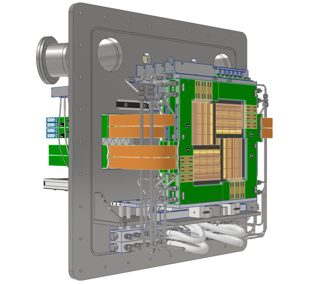
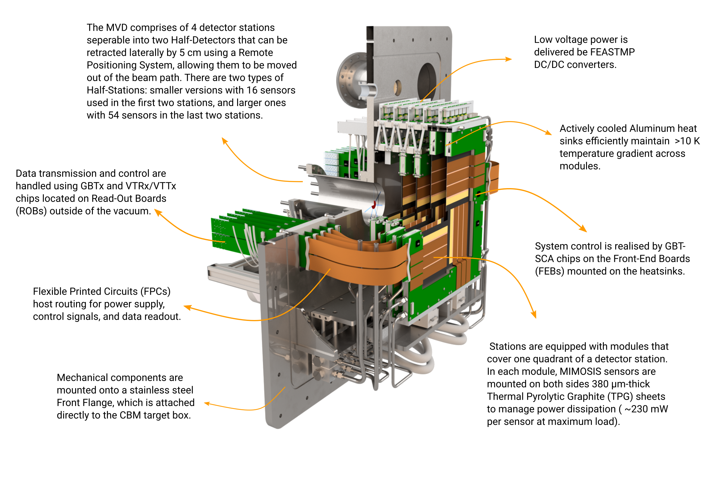
 Figure 1. CAD model of the CBM Micro Vertex Detector (MVD).
|
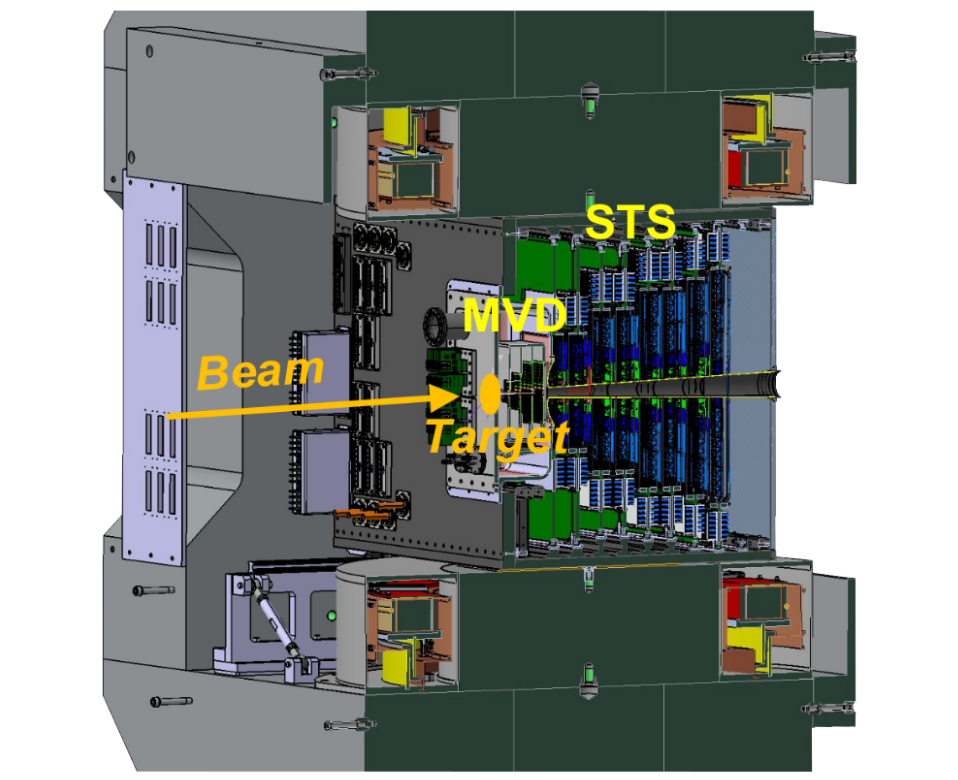
The CMOS-MAPS-based Micro Vertex Detector (MVD) is the first detector subsystem positioned downstream of the target in the CBM experiment, inside the target vacuum box. It is located between 5 to 20 cm and forms, together with the µ-strip Silicon Tracking System (STS), the CBM Silicon Tracker, positioned inside the CBM magnet. The primary goal of the MVD is to offer high-precision track reconstruction for charged particles, extending the detection range to low momenta down to a few hundreds of MeV/c. The MVD enables precise secondary-vertex reconstruction for the identification of weakly decaying charged hyperons produced in A+A collisions and open charm mesons in p+A collisions in the SIS-100 energy regime, with a precision better than 100 μm along the beam axis for decay products with laboratory momenta above 1 GeV/c. In addition, it assists in background rejection for dielectron analyses through topological cuts that suppress contributions from π0-Dalitz decays and photon conversion pairs.
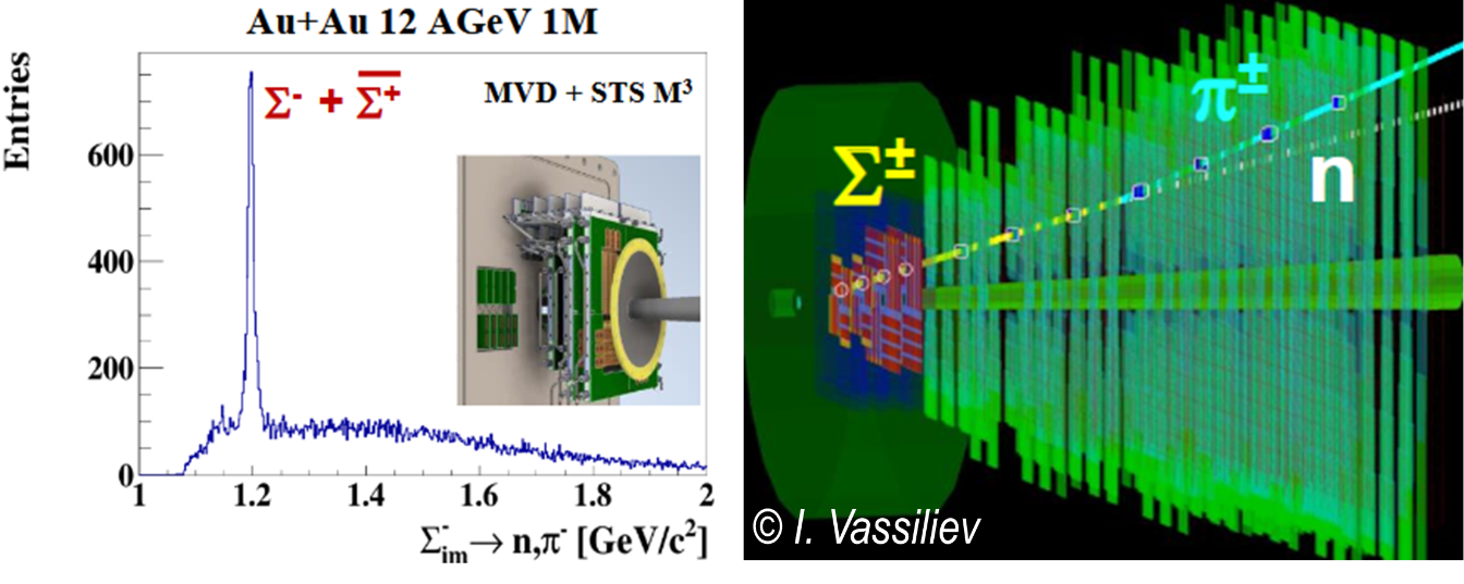 Figure 2. Reconstruction of short-lived strange hyperons with the MVD and STS. Precise secondary-vertex reconstruction enables a clear Σ signal in the invariant-mass spectrum of its decay products, even in the high-multiplicity environment of Au+Au collisions.
|
Design Criteria
|
The Micro Vertex detector is designed under rigorous constraints shaped by the need for high-precision vertexing and tracking of particles down to small laboratory momenta in the CBM energy regime. A central design objective is the reduction of the material budget to a limit of 0.3 – 0.5 x/X0 for each station, together with vacuum-compatible sensor- and detector-integration. In addition, the detector is placed inside the magnet (Integral (𝐵 𝑑𝑧) = 1 Tm). The most irradiated sensors have to withstand intense radiation: After already one CBM year the most exposed sensors can accumulate the end-of-lifetime (EOL) dose (5 MRad ionizing and 7 × 10¹³ neq/cm2 non-ionizing). This environment makes radiation hardness a critical requirement for the choice of materials as well as for the sensing element (the MIMOSIS sensor). In order to maintain high detection efficiency, suppress fake hits and control leakage current the sensors demand a stable temperature-controlled environment with a baseline operation temperature of 15 °C. Consequently thermal management poses major technical challenges, addressed by:
In summary, for CBM high-precision tracking in immediate neighborhood to the target calls for employing irradiation-hard pixel sensors and dedicated high-performance materials, while respecting vacuum operation and minimizing the overall material budget. High-granular CMOS-MAPS (MIMOSIS) thinned to 50 µm and mounted on TPG and read-out by ultra-thin flex cables represent the key design features of the CBM MVD. |
|
MVD Technical Details
|
Positioning & Environment
Geometry & Structure
Performance
|
MVD MIMOSIS
|

MVD Integration
|
|
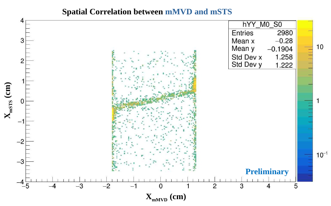
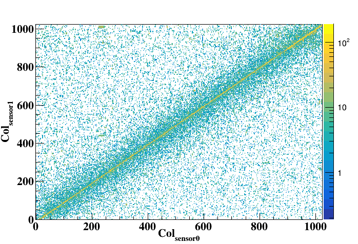
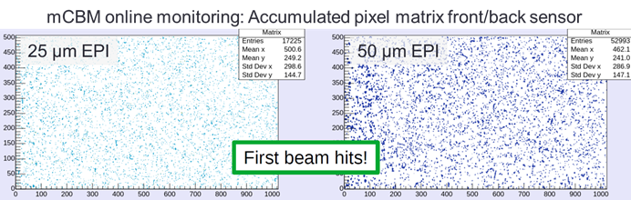
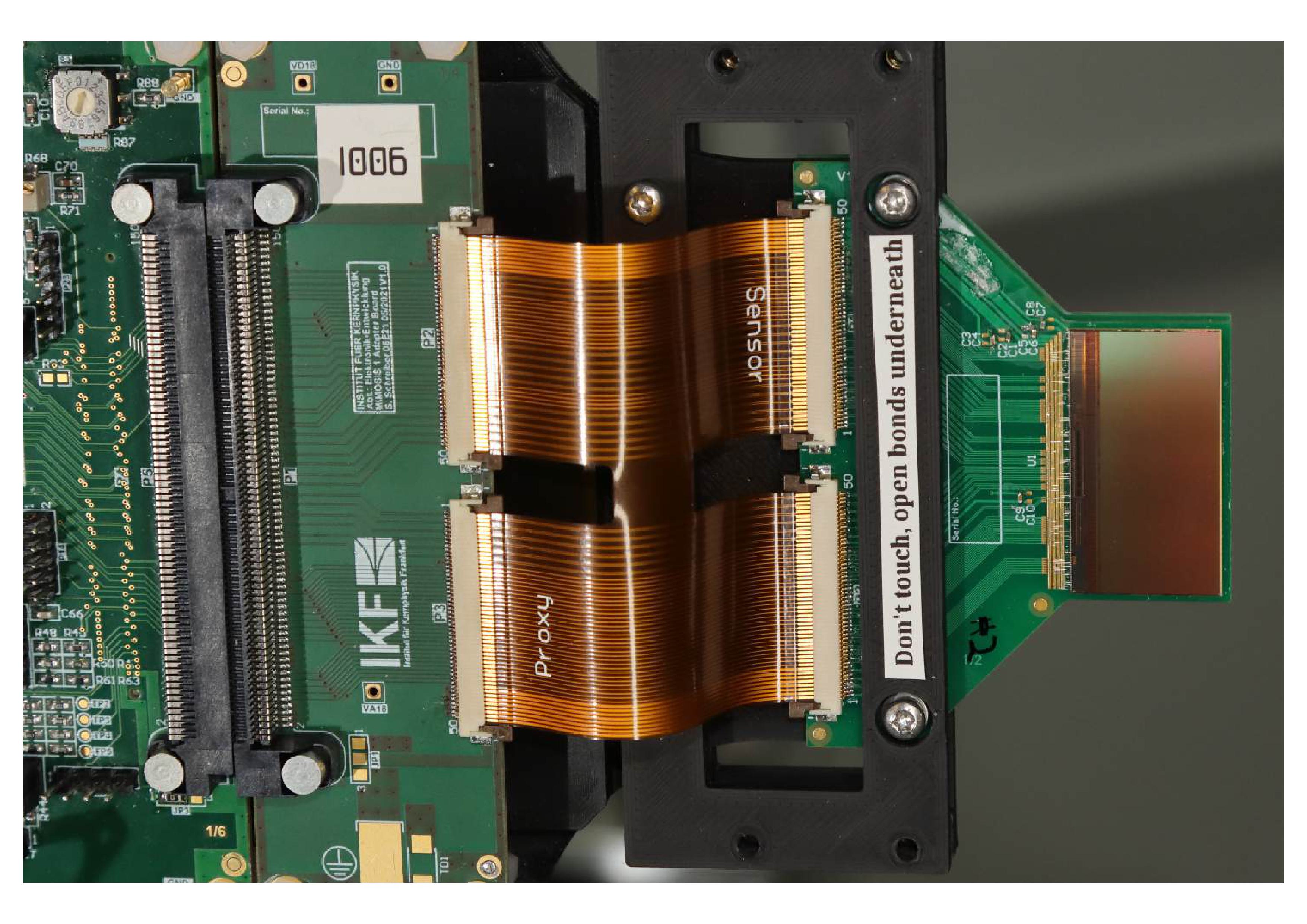
mMVD
|
In May 2025, the mMVD(mini MVD) detector module was successfully integrated for the first time into the mCBM setup. The mMVD comprises two MIMOSIS-2.1 sensors (25 and 50 µm epitaxial layer thickness) mounted back-to-back, featuring sensor-to-sensor tracking. The goal of this integration was to:
|